

Research Emphasis
-
Thin Films Deposition
-
Surface Functionnalization for Biosensors and BioMEMS
-
Microfabrication and Microtechnology Processes
-
Plasma Study and Diagnostics
Thin Films Deposition |
-
Deposition of Plasma Polymerized Allylmaine by rfGD Plasma Reactor
 |
 |
||
|
|||
-
Deposition of Plasma Polymerized TMDS by RPECVD Plasma Reactor
Under Construction
Surface Functionnalization for Biosensors and BioMEMS |
Covalent attachment of trypsin on plasma polymerized allylamine
 |
 |
||
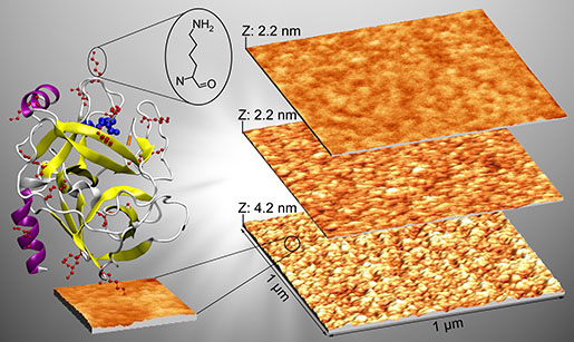
Covalent attachment of trypsin on plasma polymerized allylamineWe have developped a successful immobilization protocol of trypsin on plasma polymerized allylamine films. In particular, we c
onduct an interface analysis following the immobilization steps. All the characterization techniques used in this work (AFM, XPS, absorption spectroscopy) combinedwith the enzyme activity measurements by fluorescent spectroscopy converge to give conclusive proof of three main results: first, all the treated samples, without or with a GA linker display a complete surface coverage with a protein monolayer. This suggests that ppAA represents an interesting carrier for biomolecules immobilization, either by simple adsorpt
ion or through covalent attachment. Secondly, the glutaraldehyde cross-linking does not change significantly the amount of bound |
|||
Microfabrication and Microtechnology Processes |
-
Microfabrication by Plasma Polymerization
 |
 |
 |
|
|
|||
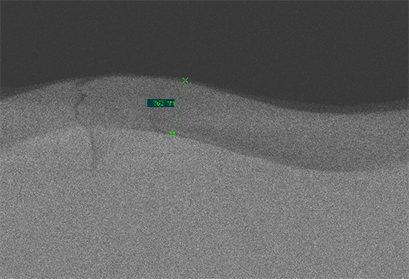
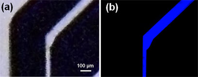
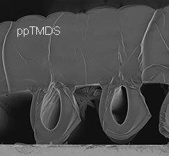
A novel fabrication method of closed microchannels for microfluidic systems is developped by our group. It is based on a direct plasma polymerization of the encapsulating material, here the organosilicon polymer ppTMDS, on a photopatterned resist. The latter, used as a sacrificial layer, was then decomposed to release the desired channels. We can easily create microchannels with various shapes and dimensions and with different surface features. In addition, this simple method allows the direct and rapid integration of fluidic circuits onto various sensors such as microelectrodes and waveguides. Applying the concept of plasma polymerization to the fluidic MEMS fabrication is particularly attractive for several reasons: (1) it avoids the bonding step in the fabrication protocol; (2) it uses the ambient temperature process; (3) the large panel of organic or organosilicon materials that can be deposited; (4) the good biocompatibility of these materials and their easy functionalization; (5) processing onto different material substrates without the need of an adhesion layer and (6) this process can be scaled up to industrial production relatively easily. Beside this, ppTMDS films enable the fabrication of very large cavities (>700 μm) without pillars and small channels (<5 μm width) without using a sacrificial material. One of our further challenges in this issue is the creation of microfluidic networks by the direct plasma polymerization of both sacrificial and overcoat layers to achieve the whole process in the same plasma reactor. |
|||
Plasma Study and Diagnostics |
Under Construction